Market Opportunity Looms Large for microLED Technology
Blogs | Mar 23, 2022
By Anil Vijayendran, Veeco’s Vice President, Strategic Marketing
MicroLED technology offers great promise for a number of applications, with cost challenges lingering as the primary factor limiting its widespread adoption. But change is on the horizon. This post—the first of a series focused on microLED—provides an overview of the market, the technology, and its capabilities, particularly as compared with other lighting approaches.
LEDs – From Revolution Through Evolution
Light-emitting diode (LED) technology has a rich history. LEDs have been in production for decades. This year, in fact, marks the 60th anniversary of the invention of the first LED that could produce visible red light. These red diodes were invented by GE engineer Nick Holonyak Jr., for which achievement he became known as the “Father of the Visible Light-Emitting Diode.”Each decade since then produced new advancements and efficiencies in LED technology, as different materials and substrates were brought into the equation.
LEDs’ big selling point, of course, is their energy efficiency, as nearly all their energy is used to produce light, whereas incandescents give off most of their energy as heat. In recent years, traditional LEDs evolved to miniLEDs as dimensions shrank from 1mm to 100m, and applications migrated from general lighting to use in televisions. This was a boon for consumers, as heavy and cumbersome CRTs were displaced by LEDs, which, in turn began to be used (as did miniLEDs) for liquid crystal display (LCD) backlighting. Figure 1 illustrates this evolution, with microLED the next to emerge.
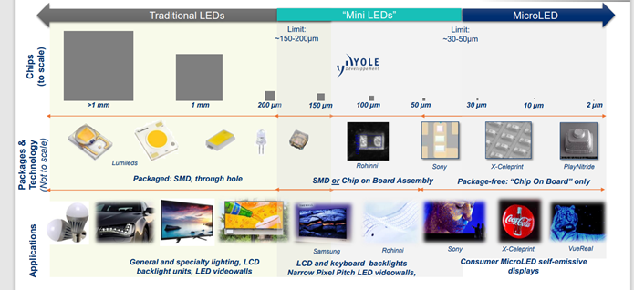
Figure 1. As chips have shrunk and packages become more sophisticated, LED technology has evolved to miniLED and now, microLED incarnations. (Source: Yole Développement)
MicroLEDs are different than their predecessors in a few key ways. First, as Figure 1 illustrates, microLEDs chips are moving to sub-5µm sizes. Second, microLED displays are self-emissive, meaning that the display generates its own light without requiring backlighting. In addition, unlike LEDs or miniLEDS, microLEDs are not individually packaged, using instead the chip-on-board (COB) approach, in which the device is mounted directly onto a substrate, e.g., silicon or sapphire. These characteristics enable microLEDs to exhibit superior image quality with respect to contrast and brightness compared with its predecessors.
Figure 2 provides a comparison of microLED’s advantages over OLED and LCD. Compared to LCDs, OLEDs and microLEDs are emissive displays, i.e., they are composed of individual pixels generating their own light, yielding superior contrast and brightness. MicroLEDs also offer higher performance than the other technologies in terms of pixel density, brightness, and contrast. This is particularly critical for applications such as augmented reality (AR).
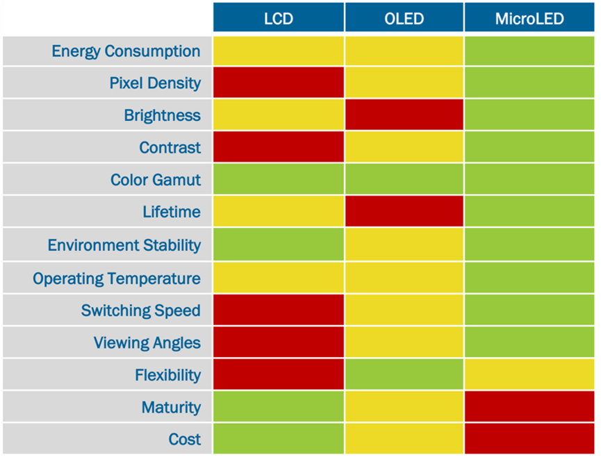
Figure 2. microLEDs offer a wealth of advantages over OLEDs and LCDs, but their cost and maturity issues must be solved to enable broad adoption.
MicroLED is significantly brighter than OLED, which is vital for creating well-lit environments. An interim step is to replace the traditional backlight with an array of miniLEDs for local dimming and improved contrast. In addition, microLEDs have the potential to offer superior lifetime, stability, operating temperature and switching speed compared with the other approaches. OLEDs’ lifetime is approximately 10,000 hours, whereas microLEDs can last up to 30,000 hours, and, unlike OLEDs, they don’t require encapsulation to withstand environmental forces such as humidity and temperature.
While microLEDs’ advantages are many, OLEDs offer better flexibility. However, the main disadvantages of microLEDs are their cost and maturity. The technology can offer tremendous advantages, and there is a path to reach volume production. However, some significant challenges need to be overcome.
microLED Opportunity and Applications
Because microLED adoption is limited by cost, the first applications to adopt the technology will be those with higher performance standards that can support the higher cost points and lower volumes for adoption, as shown in Figure 3. At left is a potential progression of microLED adoption by application, from least to most price sensitive. AR and automotive applications are the least price sensitive with the highest requirements for brightness, contrast, and durability and therefore the most immediate candidates for implementing microLED technology.
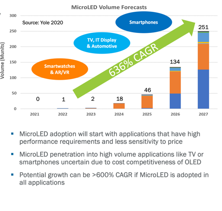
Figure 3. The potential for massive growth in the microLED exists as the trajectory moves toward less price-sensitive end products.
With the move into higher-volume consumer devices, end products grow increasingly sensitive to price, which, in turn, is likely to impact microLED adoption. Smartwatches demand high brightness and smaller form factor, as do high-end consumer TVs, which are much more price sensitive. OLED is a strong competitor to microLED in both of these markets. High volumes in smartphones and laptops could potentially push microLED adoption into the stratosphere, but their extreme price sensitivity will heighten the challenge—particularly with laptops and tablets, for which LCD and OLED currently meet display quality and contrast requirements.
The chart at the right in Figure 3 demonstrates that microLED has the potential to be a massive market, based on the application adoption path, especially as higher-volume consumer products move to these displays. Over the next few years, the technology could achieve CAGR growth as high as 636% if adoption penetrates all applications.
To achieve this will require new manufacturing approaches that reduce complexity and help boost microLED toward greater maturity. In upcoming posts, we’ll delve into process flows, innovations, and critical manufacturing challenges, and we’ll examine how Veeco’s approach to microLED manufacturing contributes to device uniformity, performance, and cost improvements.